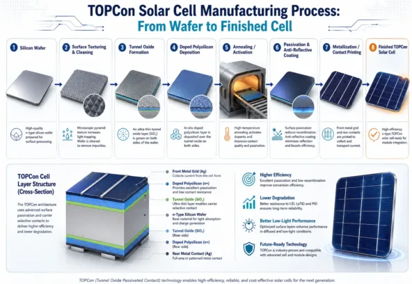

Understanding how a TOPCon cell is actually made — not just what it does once installed — matters if you’re evaluating suppliers, auditing quality processes, or simply trying to understand why certain manufacturers produce more consistent cells than others. Here’s the production process broken down step by step.
Starting Point: The N-Type Wafer
Every TOPCon cell begins with an n-type monocrystalline silicon wafer — typically phosphorus-doped, in contrast to the boron-doped p-type wafers used in older PERC production. This starting material already carries some of TOPCon’s eventual performance advantages, since n-type silicon has inherently lower bulk recombination rates than p-type material, independent of anything done to it later in the process.
Step 1: Surface Texturing
The wafer surface is textured — typically using an alkaline etching process — to create a micro-textured surface that reduces light reflection and increases the amount of sunlight absorbed into the cell rather than bounced away. This step is largely shared with PERC processing and doesn’t differ significantly between the two technologies.
Step 2: Front-Side Diffusion (Emitter Formation)
A boron diffusion process forms the front-side emitter layer, creating the p-n junction that’s fundamental to how the cell generates current from absorbed light. This is one of the few steps where TOPCon production still closely resembles standard PERC process flow, which is part of why manufacturers were able to upgrade existing PERC lines rather than build entirely new facilities.
Step 3: The Defining Step — Tunnel Oxide and Polysilicon Deposition
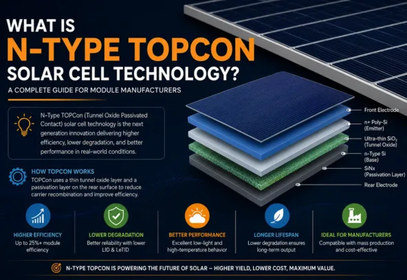
This is where TOPCon diverges fundamentally from PERC. On the rear surface of the cell, manufacturers deposit:
- An ultra-thin tunnel oxide layer, typically 1-2 nanometers thick
- A doped polysilicon layer on top of that oxide
This combination is the core innovation behind TOPCon’s name (Tunnel Oxide Passivated Contact). The oxide layer is thin enough that majority charge carriers can pass through it via quantum tunneling, while the layer still effectively passivates the rear surface — meaning it dramatically reduces the recombination losses that would otherwise occur at an unpassivated rear contact.
Two deposition approaches dominate current production: chemical vapor deposition (CVD), which is widely used across Chinese manufacturing and has matured into a cost-effective, high-throughput process; and physical vapor deposition (PVD), an alternative that some manufacturers favor because it avoids the toxic and flammable process gases associated with CVD, instead using solid-state sputtering targets. Both approaches can deliver to spec, but the choice affects a manufacturer’s safety profile, supply chain for process materials, and in some cases cost structure.
Step 4: Anti-Reflective Coating (Front Side)
A silicon nitride (SiN) anti-reflective coating is applied to the front surface, further reducing reflection losses and improving the cell’s ability to absorb usable light across the solar spectrum. This step typically uses plasma-enhanced chemical vapor deposition (PECVD), often performed in two separate steps — one for the front side, one for the rear — using automated handling systems to move cells between coating tools.
Step 5: Metallization (Screen Printing and Firing)
Metal contacts are screen-printed onto both the front and rear surfaces of the cell to collect and conduct the electrical current generated. The cell then passes through a firing furnace, which sets the metal paste and forms the electrical contacts that connect to the silicon below. Increasingly, manufacturers are exploring silver-free or reduced-silver metallization approaches to manage material costs, though silver-based pastes remain the industry standard as of 2026.
Step 6: Testing and Sorting
Finished cells go through electrical testing — measuring power output, efficiency, and electrical characteristics — and are sorted into performance bins. This sorting matters significantly for module manufacturers: cells with closely matched electrical characteristics perform better when wired together in a module string, since mismatched cells create a bottleneck effect where the weakest cell limits the output of the entire string.
Why Process Consistency Matters More Than Any Single Step
No individual step in this process is exotic or proprietary at this point — TOPCon manufacturing knowledge has spread widely across the industry since 2013. What separates a reliable supplier from an inconsistent one is process control: tight tolerances on oxide layer thickness, consistent doping concentration, stable furnace temperatures during firing, and rigorous testing before cells ship.
For module manufacturers, this means supplier evaluation should go beyond asking “do you produce TOPCon cells” and toward asking about process control documentation, defect rates, and batch-to-batch consistency data.
PTECH Solar’s Manufacturing Approach
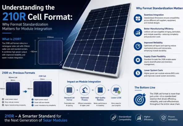
PTECH Solar produces n-type TOPCon cells in the 210R format at our facility in Düzce, Turkey, with process controls built around consistency across production batches — a priority for module manufacturers who need predictable performance characteristics for line integration and customer-facing warranties alike.
We’re glad to walk manufacturers through our specific process documentation and quality control data as part of supplier evaluation.
This article is part of PTECH Solar’s technical resource series for module manufacturers and B2B solar buyers. For questions about our N-type TOPCon 210R cells and manufacturing process, visit ptechsolar.com.