

Manufacturing Process and Quality Control Checkpoints

The manufacturing line is structured into two primary phases: Wafer Manufacturing and TOPCon Cell Production. Each stage is governed by defined process parameters and in-line quality control checkpoints to ensure product consistency, reliability, and performance.
Product Technology: TOPCon and N-Type Cells
Production Hub: The facility is designated as a “TOPCon+ Solar Cell Production Base.”
Cell Type: Manufacturing activities are primarily focused on N-type solar cells and bifacial cell technologies, whereby bifacial cells are capable of generating electrical energy from both the front and rear surfaces.
Tech Blueprint: The facility is designed to utilize TOPCon (Tunnel Oxide Passivated Contact) technology, which enables enhanced performance through tunnel oxide passivation of the contacts.
Wafer Manufacturing Line Flow
Thıs phase covers the conversIon of SILICON Ingots Into hIgh-precIsIon wafers:
Ingot bricks are bonded onto metal plates and conditioned to ensure dimensional stability prior to slicing.
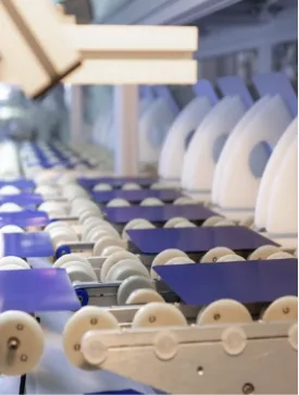
Ingots are precision-sliced into thin wafers using controlled cutting parameters.
Mechanical separation of wafers from the polymer mounting plates.
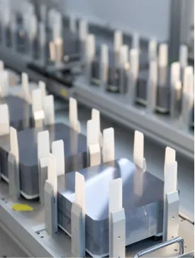
A critical quality control stage where wafers are inspected and classified based on defined dimensional, visual, and electrical quality criteria.
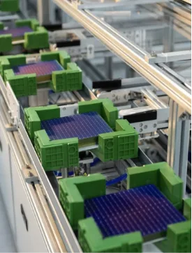
Designed packaging to safeguard quality and minimize risk of damage.
TOPCon Cell Production Line Flow
ThIs phase Involves the transformatIon of wafers Into electrIcIty-generatıng solar cells through advanced chemIcal, thermal, and deposItIon processes:
Surface texturing to optimize optical properties and enhance light absorption.
Joint formation via boron diffusion.
Removal of borosilicate glass followed by rear-surface alkaline polishing.
Low-Pressure Chemical Vapor Deposition
Phosphorus Diffusion
Phosphorus Diffusion
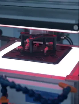
High-purity RCA cleaning followed by Atomic Layer Deposition (ALD) for precise passivation layers.
Front and rear surface SiNx (Silicon Nitride) coatings
Printing of electrical conductors (busbars)
Contact optimization using laser
At the end of production, the cells are tested and classified (the ‘Control and Classification’ area is shown on the layout)